Crystallographic NDT

Metal-working and forming processes, including casting, forging, and 3D-printing, produce metal-alloy parts with highly crystalline structures and microstructures. Most parts are polycrystalline and characterized by grains with size, shape, and crystal-orientation distributions that vary widely with the alloy and process. Manufacturing industries employ crystallographic models of physical, electrical, and optical properties of their materials and parts. The strengths and failure probabilities of structural metal parts for instance depend on their crystallographic microstructures, and verified models are mandatory for safety assurance and quality control of safety-critical parts. In addition to metals, crystallographic models are critical to manufacturing of optical and laser crystals, ceramics, semiconductor electronics, solar cells, and other crystalline devices and parts.
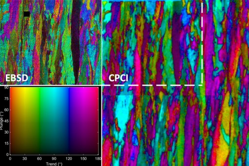
X-ray diffraction (XRD) was the first technique to regularly measure crystallographic structure over small areas, although diffracted x-rays generally cannot be refocused and recorded to produce crystallographic images. Lower-frequency electromagnetic waves, including visible light, which can obviously form images, do not diffract from crystal planes, but rather exhibit changes in their complex amplitudes upon reflection or transmission that depend on lattice spacing and orientation. Polarized light has therefore been utilized for over 80 years to image and measure the sizes and shapes of crystal grains through techniques commonly referred to as polarized-light microscopy (PLM). PLM is often considered semi-quantitative because it traditionally has not revealed crystal orientation within grains.

Electron beams diffract from crystals similarly to x-rays, and can be focused to sufficiently small probe spots to enable scanned imaging. Electron backscattering diffraction (EBSD), a specialized form of scanning electron microscopy (SEM), is the preferred technique for crystallographic orientation imaging, but has limitations that affect its broader use. EBSD is generally destructive because the part must be cut into a sample small enough to fit into an SEM vacuum chamber, EBSD data-acquisition times are long, EBSD requires highly polished surfaces, and the field-of-view (FOV) typically cannot exceed 1cm on its short side, which is significant because failure probabilities are strongly dependent on spatial correlations of crystal orientations that can extend over larger areas. A faster, less destructive, parallel technique for crystallographic orientation imaging is needed to enable application of texture models to industrial parts. AOT's CrystalView CPCI satisfies this need for certain metals and other oriented materials employed for aerospace, energy, and medical parts.